PLASMA ETCHING
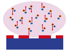
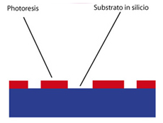
Reactive ion etching (RIE) is a dry technology and is used on almost all materials that are used in electronics and optoelectronics. Reactive ion etching (RIE) is a dry technology and is used on almost all materials that are used in electronics and optoelectronics. The substrate or sample is bombarded with charged particles that remove layer by layer from the surface, in a reproducible and anisotropic manner.
Reactive ion etching (RIE) is primarily used for anisotropic structuring of silicon, organic and inorganic dielectric materials, metallic barrier materials, and polymers for electronic and optoelectronic applications.