PLASMA ETCHING
Reactive ion attachment (RIE) is a dry technology and is used on almost all materials that are used in electronics and optoelectronics. Reactive ion etching (RIE) is a dry technology and is used on almost all materials that are used in electronics and optoelectronics. The substrate or sample is bombarded with charged particles that remove layer by layer from the surface, in a reproducible and anisotropic manner. Reactive ion attachment (RIE) is mainly used for anisotropic structuring of silicon, organic and inorganic dielectric materials, metallic barrier materials, and polymers for electronic and optoelectronic applications.
Plasma etching
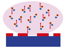
Plasma etching is one of the most advanced techniques in the field of microfabrication and nanotechnology, used for creating complex electronic circuits and components on a microscopic scale. This technology is based on the use of plasma, a state of matter where gases are ionized, meaning they are separated into positive ions and free electrons. This cold plasma state is achieved through an ionization process that occurs in a reaction chamber, where the gas is applied at low pressure and ionized using an electrical discharge.
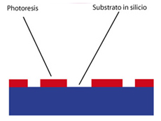
The plasma etching process stands out for its ability to create microscopic structures with incredible precision, essential for the production of electronic chips, semiconductor devices, and other small electronic components. Plasma etching can work with a variety of materials, including silicon, oxides, metals, and polymers, thanks to its ability to select specific chemical reactions between the plasma and the starting material. This enables localized removal of material without damaging other areas of the substrate.
One of the main applications of plasma etching is in the production of integrated circuits (IC). During the fabrication of an IC, plasma etching is used to remove thin layers of material from a silicon wafer, creating very fine electronic circuits. The advantages of this technique are numerous: in addition to precise dimensions, it allows working on very complex substrates, minimizing the risk of errors.
The plasma etching process can be divided into several stages: the first is material preparation, where the material is placed in a low-pressure chamber. Then, the process gas, which can be a mix of various gases such as oxygen, chlorine, or fluorine, is introduced into the chamber. The plasma generated through the electrical discharge reacts with the material, forming reactive species that selectively attack the surface. The chemical reaction that occurs is precisely controlled to achieve the desired structure.
In addition to its application in electronics, plasma etching is also used in the nanotechnology sector, in the production of MEMS devices, and in applications such as the fabrication of sensors, microvalves, and pressure sensors. The precise control of process conditions, such as temperature, pressure, and gas flow, is crucial for achieving optimal results, as well as for ensuring the repeatability of the process on a large scale.
In conclusion, plasma etching is a fundamental technology for the evolution of electronics and nanotechnology, as it enables the production of smaller and more complex devices, with applications ranging from medicine to industrial automation. The continuous improvement of dry etching systems, plasma etchers, and plasma products, as well as innovation in gases and process control methods, are pushing the boundaries of what is possible in technological advancements.